1. Fundamental Features and Nanoscale Actions of Silicon at the Submicron Frontier
1.1 Quantum Confinement and Electronic Structure Transformation
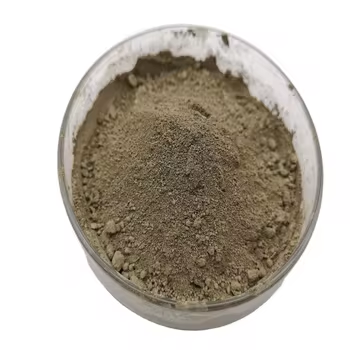
(Nano-Silicon Powder)
Nano-silicon powder, composed of silicon bits with particular dimensions listed below 100 nanometers, stands for a standard change from bulk silicon in both physical habits and useful utility.
While mass silicon is an indirect bandgap semiconductor with a bandgap of approximately 1.12 eV, nano-sizing causes quantum confinement results that basically modify its electronic and optical properties.
When the bit diameter approaches or falls listed below the exciton Bohr distance of silicon (~ 5 nm), cost service providers end up being spatially constrained, bring about a widening of the bandgap and the appearance of noticeable photoluminescence– a sensation missing in macroscopic silicon.
This size-dependent tunability allows nano-silicon to produce light throughout the visible range, making it an appealing prospect for silicon-based optoelectronics, where conventional silicon fails as a result of its bad radiative recombination effectiveness.
Additionally, the enhanced surface-to-volume ratio at the nanoscale improves surface-related sensations, including chemical reactivity, catalytic task, and interaction with electromagnetic fields.
These quantum effects are not merely academic curiosities yet develop the structure for next-generation applications in power, noticing, and biomedicine.
1.2 Morphological Variety and Surface Chemistry
Nano-silicon powder can be manufactured in different morphologies, consisting of spherical nanoparticles, nanowires, permeable nanostructures, and crystalline quantum dots, each offering distinctive advantages depending upon the target application.
Crystalline nano-silicon normally retains the ruby cubic structure of mass silicon but shows a higher thickness of surface area flaws and dangling bonds, which need to be passivated to maintain the product.
Surface area functionalization– usually accomplished through oxidation, hydrosilylation, or ligand accessory– plays a crucial function in figuring out colloidal security, dispersibility, and compatibility with matrices in composites or biological environments.
For instance, hydrogen-terminated nano-silicon shows high sensitivity and is susceptible to oxidation in air, whereas alkyl- or polyethylene glycol (PEG)-layered bits show enhanced stability and biocompatibility for biomedical use.
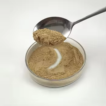
( Nano-Silicon Powder)
The existence of a native oxide layer (SiOₓ) on the particle surface area, even in very little amounts, significantly affects electrical conductivity, lithium-ion diffusion kinetics, and interfacial reactions, particularly in battery applications.
Recognizing and managing surface chemistry is therefore crucial for utilizing the full possibility of nano-silicon in useful systems.
2. Synthesis Techniques and Scalable Construction Techniques
2.1 Top-Down Approaches: Milling, Etching, and Laser Ablation
The production of nano-silicon powder can be generally classified right into top-down and bottom-up approaches, each with distinctive scalability, pureness, and morphological control features.
Top-down strategies involve the physical or chemical decrease of bulk silicon into nanoscale fragments.
High-energy ball milling is a widely made use of commercial technique, where silicon chunks go through extreme mechanical grinding in inert environments, leading to micron- to nano-sized powders.
While cost-effective and scalable, this method usually introduces crystal flaws, contamination from crushing media, and wide fragment size distributions, needing post-processing purification.
Magnesiothermic reduction of silica (SiO ₂) followed by acid leaching is another scalable route, especially when making use of natural or waste-derived silica sources such as rice husks or diatoms, offering a lasting path to nano-silicon.
Laser ablation and reactive plasma etching are a lot more specific top-down techniques, with the ability of generating high-purity nano-silicon with controlled crystallinity, however at greater expense and reduced throughput.
2.2 Bottom-Up Approaches: Gas-Phase and Solution-Phase Development
Bottom-up synthesis enables higher control over particle dimension, form, and crystallinity by building nanostructures atom by atom.
Chemical vapor deposition (CVD) and plasma-enhanced CVD (PECVD) allow the development of nano-silicon from gaseous forerunners such as silane (SiH FOUR) or disilane (Si two H SIX), with parameters like temperature level, pressure, and gas circulation determining nucleation and growth kinetics.
These methods are especially effective for creating silicon nanocrystals embedded in dielectric matrices for optoelectronic tools.
Solution-phase synthesis, including colloidal courses utilizing organosilicon substances, enables the production of monodisperse silicon quantum dots with tunable emission wavelengths.
Thermal decomposition of silane in high-boiling solvents or supercritical liquid synthesis likewise yields top quality nano-silicon with narrow size distributions, ideal for biomedical labeling and imaging.
While bottom-up approaches typically generate exceptional worldly top quality, they face obstacles in massive manufacturing and cost-efficiency, necessitating continuous study right into crossbreed and continuous-flow procedures.
3. Energy Applications: Changing Lithium-Ion and Beyond-Lithium Batteries
3.1 Function in High-Capacity Anodes for Lithium-Ion Batteries
One of the most transformative applications of nano-silicon powder hinges on power storage, specifically as an anode product in lithium-ion batteries (LIBs).
Silicon offers a theoretical certain capacity of ~ 3579 mAh/g based upon the formation of Li ₁₅ Si ₄, which is almost 10 times more than that of standard graphite (372 mAh/g).
Nonetheless, the big volume expansion (~ 300%) throughout lithiation causes fragment pulverization, loss of electric contact, and continuous solid electrolyte interphase (SEI) formation, resulting in fast ability fade.
Nanostructuring mitigates these issues by shortening lithium diffusion paths, fitting pressure more effectively, and reducing fracture chance.
Nano-silicon in the form of nanoparticles, permeable structures, or yolk-shell structures makes it possible for relatively easy to fix biking with improved Coulombic effectiveness and cycle life.
Industrial battery technologies now include nano-silicon blends (e.g., silicon-carbon compounds) in anodes to increase energy thickness in consumer electronic devices, electric automobiles, and grid storage space systems.
3.2 Possible in Sodium-Ion, Potassium-Ion, and Solid-State Batteries
Past lithium-ion systems, nano-silicon is being checked out in arising battery chemistries.
While silicon is less responsive with sodium than lithium, nano-sizing enhances kinetics and enables minimal Na ⁺ insertion, making it a candidate for sodium-ion battery anodes, specifically when alloyed or composited with tin or antimony.
In solid-state batteries, where mechanical stability at electrode-electrolyte interfaces is critical, nano-silicon’s capacity to go through plastic contortion at tiny ranges lowers interfacial stress and anxiety and enhances call upkeep.
Additionally, its compatibility with sulfide- and oxide-based strong electrolytes opens avenues for safer, higher-energy-density storage space solutions.
Research study remains to maximize user interface design and prelithiation approaches to take full advantage of the longevity and efficiency of nano-silicon-based electrodes.
4. Emerging Frontiers in Photonics, Biomedicine, and Composite Materials
4.1 Applications in Optoelectronics and Quantum Light
The photoluminescent residential properties of nano-silicon have rejuvenated efforts to develop silicon-based light-emitting devices, a long-lasting obstacle in integrated photonics.
Unlike bulk silicon, nano-silicon quantum dots can display effective, tunable photoluminescence in the noticeable to near-infrared range, making it possible for on-chip lights compatible with corresponding metal-oxide-semiconductor (CMOS) modern technology.
These nanomaterials are being integrated into light-emitting diodes (LEDs), photodetectors, and waveguide-coupled emitters for optical interconnects and noticing applications.
In addition, surface-engineered nano-silicon shows single-photon discharge under specific flaw setups, positioning it as a possible system for quantum information processing and secure interaction.
4.2 Biomedical and Ecological Applications
In biomedicine, nano-silicon powder is getting interest as a biocompatible, naturally degradable, and non-toxic alternative to heavy-metal-based quantum dots for bioimaging and drug shipment.
Surface-functionalized nano-silicon particles can be created to target particular cells, release therapeutic representatives in response to pH or enzymes, and offer real-time fluorescence tracking.
Their deterioration right into silicic acid (Si(OH)₄), a naturally happening and excretable substance, decreases long-lasting toxicity problems.
Additionally, nano-silicon is being checked out for ecological remediation, such as photocatalytic degradation of contaminants under visible light or as a minimizing agent in water treatment processes.
In composite materials, nano-silicon enhances mechanical toughness, thermal stability, and put on resistance when incorporated right into metals, ceramics, or polymers, particularly in aerospace and automotive components.
To conclude, nano-silicon powder stands at the crossway of essential nanoscience and industrial technology.
Its distinct combination of quantum effects, high reactivity, and convenience across energy, electronic devices, and life scientific researches highlights its role as an essential enabler of next-generation innovations.
As synthesis techniques development and integration difficulties relapse, nano-silicon will certainly continue to drive progression toward higher-performance, lasting, and multifunctional material systems.
5. Vendor
TRUNNANO is a supplier of Spherical Tungsten Powder with over 12 years of experience in nano-building energy conservation and nanotechnology development. It accepts payment via Credit Card, T/T, West Union and Paypal. Trunnano will ship the goods to customers overseas through FedEx, DHL, by air, or by sea. If you want to know more about Spherical Tungsten Powder, please feel free to contact us and send an inquiry(sales5@nanotrun.com).
Tags: Nano-Silicon Powder, Silicon Powder, Silicon
All articles and pictures are from the Internet. If there are any copyright issues, please contact us in time to delete.
Inquiry us